Wetenschap
Vloeibare cel transmissie elektronenmicroscopie analyse van halfgeleider nanokristallen
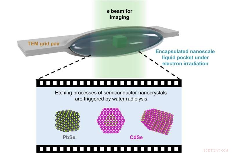
Illustratie van de LCTEM-experimenten. De dwarsdoorsnede laat zien dat een dunne waterige laag met halfgeleider nanokristallen is ingeklemd tussen twee ultradunne koolstoffilms van een paar TEM-roosters. De elektronenstraal die door het water en de koolstoflagen gaat, veroorzaakt radiolysereacties in het water, die vervolgens de etstrajecten activeren die met LCTEM worden afgebeeld. Krediet:Wetenschappelijke vooruitgang (2022). DOI:10.1126/sciadv.abq1700
Halfgeleider nanokristallen van verschillende groottes en vormen kunnen de optische en elektrische eigenschappen van materialen bepalen. Vloeibare celtransmissie-elektronenmicroscopie (LCTEM) is een opkomende methode om chemische transformaties op nanoschaal te observeren en de precieze synthese van nanostructuren met verwachte structurele kenmerken te informeren. Onderzoekers onderzoeken de reacties van halfgeleider nanokristallen met de methode om de zeer reactieve omgeving te bestuderen die tijdens het proces wordt geproduceerd via vloeibare radiolyse.
In een nieuw rapport dat nu is gepubliceerd in Science Advances , Cheng Yan en een onderzoeksteam in Chemistry and Materials Science aan de University of California Berkeley, en het Leibniz Institute of Surface Engineering, Duitsland, gebruikten het radiolyseproces om het etstraject van enkelvoudige deeltjes van prototypische halfgeleider-nanomaterialen te vervangen. Loodselenide-nanobuisjes die tijdens het werk werden gebruikt, vertegenwoordigden een isotrope structuur om de kubische vorm voor etsen te behouden via een laag-voor-laag-mechanisme. De anisotrope pijlvormige cadmiumselenide-nanostaafjes behielden polaire facetten met cadmium- of seleniumatomen. De trajecten van transmissievloeistofcelelektronenmicroscopie onthulden hoe de reactiviteit van specifieke facetten in vloeibare omgevingen de vormtransformaties van halfgeleiders op nanoschaal beheersten.
Optimaliseren van vloeistofceltransmissie-elektronenmicroscopie (LCTEM)
Halfgeleider nanokristallen bevatten breed afstembare optische en elektrische eigenschappen die afhankelijk zijn van hun grootte en vorm voor een breed scala aan toepassingen. Materiaalwetenschappers hebben de reactiviteit van specifieke bulkkristalfacetten op groei- en etsreacties gekarakteriseerd om de meest willekeurige patronen te ontwikkelen in top-down bulkhalfgeleiderverwerking. De meerdere facetten van nanokristallen en hun reactiemechanisme maken ze interessant voor direct onderzoek. De thermodynamica van colloïdale nanokristallen kan de organisch-anorganische interfaces beïnvloeden die ze definiëren. Transmissie-elektronenmicroscopie met vloeibare cellen biedt de vereiste ruimte-tijdresolutie om dynamiek op nanoschaal te observeren, zoals het zelfassemblageproces. Het team plaatste daarom een waterige zak met nanokristallen tussen de ultradunne koolstoflagen van twee transmissie-elektronenmicroscopieroosters en gebruikte tris (hydroxymethyl) aminomethaanhydrochloride (tris·HCl), een organisch molecuul om het etsen van gevoelige halfgeleider nanokristallen te reguleren.
Bestaand onderzoek naar LCTEM en nanokristallen is beperkt tot edelmetalen vanwege hun onvermogen om de chemische omgeving tijdens radiolyse te reguleren, waardoor reactieve materialen worden afgebroken. Recent onderzoek suggereert een mogelijkheid om nieuwe omgevingen voor LCTEM te ontwerpen, om etstrajecten van enkelvoudige deeltjes van reactieve nanokristallen te observeren. Tijdens de experimenten reguleerde het tris·HCl-additief het elektrochemische potentieel van het etsproces, en het team gebruikte kinetische modellering om de concentratie en het elektrochemische potentieel van de amineradicalen in de vloeibare cel te schatten.
Proof-of-concept
Als proof of concept verkregen de wetenschappers representatieve transmissie-elektronenmicroscopiebeelden van een loodselenide-nanokubus in vacuüm en verzamelden een tijdreeks van beelden tijdens laag-voor-laag etsen van loodselenide-nanokristallen. The outcome of LCTEM imaging showed the formation of a substance with higher image contrast around the lead selenide nanocrystals as a product of etching reactions, it appears that during the etching process, selenium oxidized and dispersed into the liquid to facilitate the formation of lead chloride, with chloride ions in the lead pocket. When compared to the cubic lattice of lead selenide, wurzite cadmium selenide featured an anisotropic lattice with alternating layers of cadmium and selenium atoms. During the growth of wurzite cadmium selenide nanocrystals, the surfactant ligands favorably bound to the cadmium regions to facilitate the fast growth of selenium regions.
Yan et al. presented the structure of cadmium selenide nanorods resolved via high-angle annular dark field scanning transmission electron microscopy in vacuum. The scientists generated the images by collecting electrons scattered to high angles by atoms in the material to develop mass-thickness image contrast, where cadmium was brighter than selenium. The team similarly performed in situ etching experiments on arrow-shaped cadmium selenide nanorods.
-
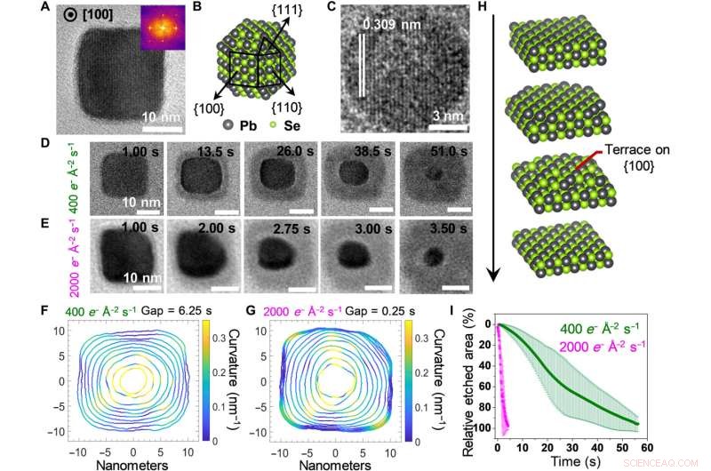
Structural characterization and etching trajectories of PbSe nanocubes. (A) Representative static TEM image of a PbSe nanocube oriented along the [100] zone axis. (B) Atomistic model of a truncated PbSe nanocube exposing different facets. (C) The LCTEM image captured near the end of an etching trajectory, exhibiting the characteristic d-spacing of {200} lattice planes of PbSe. (D and E) Time-lapse LCTEM images recorded at the electron fluence rates of 400 e− Å−2 s−1 (D) and 2000 e− Å−2 s−1 (E), respectively. (F and G) Outlines of the nanocrystals plotted with equal time gaps for illustrating the evolving shapes and local curvatures of PbSe nanocrystals recorded at 400 e− Å−2 s−1 (F) and 2000 e− Å−2 s−1 (G), respectively. (H) Scheme of the layer-by-layer etching mechanism, which proceeds via terrace intermediates. (I) The time-dependent plots of the relative etched area normalized to the projected area of the PbSe nanocube at the starting frame. Krediet:Wetenschappelijke vooruitgang (2022). DOI:10.1126/sciadv.abq1700
-
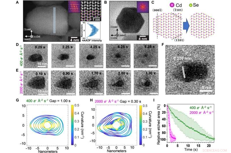
Structural characterization and etching trajectories of CdSe nanorods. (A) AC-HAADF-STEM image of a wurtzite CdSe nanorod projected along the [110] zone axis (left). The enlarged inset (top right) verifies the polarity of the nanorod:The tip of the rod is terminated by Se (green), while the bottom is terminated by Cd (pink). The line profile of HAADF-STEM intensity in the shaded segment (left) projected along the [00] axis is included in the bottom right. (B) TEM image of a nanorod oriented along the c axis showing a hexagonal projection. (C) Lattice models of a CdSe nanorod projected along the [110] axis (left) and the truncated structure (right) formed by selectively etching the Se-terminated facets. (D and E) Time-lapse LCTEM images recorded at electron fluence rates of 400 e− Å−2 s−1 (D) and 2000 e− Å−2 s−1 (E), respectively. (F) The LCTEM image exhibiting the characteristic d-spacing of {0002} lattice planes. (G and H) Outlines of the nanocrystals plotted with equal time gaps for illustrating the evolving shapes and local curvatures of CdSe nanorods at 400 e− Å−2 s−1 (G) and 2000 e− Å−2 s−1 (H), respectively. (I) Time-dependent plots of the relative etched area normalized to the projected area of the CdSe nanorod at the starting frame. Krediet:Wetenschappelijke vooruitgang (2022). DOI:10.1126/sciadv.abq1700
The etching trajectory of a wurtzite CdSe nanocrystal viewed along the [000] axis. (A) Time-lapse LCTEM images recorded at 400 e− Å−2 s−1. (B) Atomistic model of the CdSe nanocrystal with the (000) facet pointing up. (C) Time-dependent plot of the average electron fluence rates detected in different color-coded segments (inset) of the LCTEM images. Gray color corresponds to the background region surrounding the nanocrystal. (D) 3D illustration of the etching process showing that the selective etching of the Se-terminated (000) facet causes the tip to transform into a concave pit in the nanocrystal. Krediet:Wetenschappelijke vooruitgang (2022). DOI:10.1126/sciadv.abq1700
In this way, Cheng Yan and colleagues used liquid cell electron microscopy (LCTEM) to show the possibility of directly examining the facet-dependent reactivity of colloidal nanocrystals at the nanoscale. The method offered real-time, continuous structural trajectories, in contrast to classical methods. Existing research had already highlighted the effect of the inclusion or removal of ligands on the self-assembly and etching of nanocrystals in LCTEM experiments.
The team showed how sensitive nanomaterials such as lead selenide can be studied using LCTEM and highlighted the inclusion of organic additives such as tris·HCl to regulate the radiolytic redox environment in liquid cell electron microscopy. Future studies can enable the potential to gain real-time information about the transformation of an array of functional nanostructures with increasing complexity using core/shell nanocrystals, as well as those assembled via inorganic-organic interfaces. + Verder verkennen
How gas nanobubbles accelerate solid-liquid-gas reactions
© 2022 Science X Network
 Klimaatwetenschappers proberen hun eigen ecologische voetafdruk te verkleinen
- Versneld drogen verhoogt de kans op bosbranden in de hele staat in Texas
- Wat zijn de windsnelheden in een tropisch regenwoud?
- Ontdekking van ontvlambaar ijs biedt aanwijzingen voor leven op andere planeten
- Noodtoestand uitgeroepen in door tyfoon geteisterde Noordelijke Marianen
Hoofdlijnen
- Great Basin zaadstudie-experiment richt zich op herstel van weidegronden
- Mutatie in belangrijke moleculen kan gonorroe-infectie stoppen
- Bron van Beperking Enzymes
- Wat is de brugfase van glycolyse?
- Twee soorten spitssnuitdolfijnen duren erg lang, diepe duiken voor hun grootte
- Hoe gaan ziekten van de ene soort naar de andere?
- Wat gebeurt er op een microscopisch niveau tijdens homeostase?
- Eerste mycobiome-atlas beschrijft associaties tussen kanker en schimmels
- Nieuw onderzoek identificeert een gebrek aan geschikte bestrijdingsmiddelen voor veel belangrijke infectieziekten bij dieren
- Probe maakt tumoronderzoek mogelijk met behulp van complementaire beeldvormingstechnieken
- Plasmonen geactiveerd in kwantumputten van nanobuisjes
- Zenuwwikkelend nanovezelgaas dat regeneratie bevordert
- Nieuwe hybride microscoop biedt ongeëvenaarde mogelijkheden
- Nano-machinewinkel vormt nanodraden, ultradunne films

 Groene oplosmiddelen vinden voor gedrukte elektronica
- Katalytische koppelingen begrijpen:niet alle synergieën zijn eenvoudig
- Kwantumkritische geleidbaarheid van de Dirac-vloeistof in grafeen
- Astronomen zien tekenen van samensmelting van superzware zwarte gaten
- NASA introduceert online toolkit om commercieel gebruik van satellietgegevens te promoten
- Luchtvaartmaatschappijen in Azië-Pacific kunnen 27,8 miljard dollar verliezen door coronavirus:IATA
- Een vereenvoudigd nieuw proces zet houtafval uit landbouw en bosbeheer om in ethanol
- Groen cement een stap dichter bij een game-changer voor bouwemissies
- Elektronica
- Biologie
- Zonsverduistering
- Wiskunde
- French | Italian | Spanish | Portuguese | Swedish | German | Dutch | Danish | Norway |

-
Wetenschap © https://nl.scienceaq.com
