Wetenschap
Dun mica vertoont halfgeleidend gedrag, zeggen wetenschappers in nieuw onderzoek
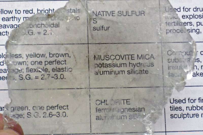
Moskoviet mica (MuM) is een gelaagd mineraal dat gewoonlijk als isolator wordt gebruikt. In een nieuwe studie merkten onderzoekers op dat MuM, wanneer het wordt verdund tot een paar molecuullagen, meer als een halfgeleider werkt met een dikteafhankelijke geleidbaarheid. Krediet:James St. John
Mica, een bekende isolator, blijkt zich als een halfgeleider te gedragen wanneer het wordt verdund tot een paar moleculaire lagen
Moskoviet mica (MuM) is een zeer stabiel mineraal dat vaak wordt gebruikt als isolator. De elektrische eigenschappen van enkellaags en weiniglaags MuM zijn echter niet goed begrepen. Nu rapporteert en verklaart een groep onderzoekers uit Japan en India een ongewoon hoge geleidbaarheid in MuM-vlokken die slechts enkele molecuullagen dik zijn. Hun bevindingen kunnen deuren openen naar de ontwikkeling van tweedimensionale elektronische apparaten die bestand zijn tegen ruwe omgevingen.
In 2004 gebruikten onderzoekers van de Universiteit van Manchester plakband om vellen enkele koolstofatomen weg te trekken van grafiet om grafeen te maken - een materiaal dat 1000 keer dunner is dan mensenhaar maar sterker dan staal. Deze baanbrekende exfoliatietechniek maakte de weg vrij voor de ontwikkeling van een breed scala aan tweedimensionale materialen met verschillende elektrische en fysieke kenmerken voor de volgende generatie elektronische apparaten.
Een dergelijk materiaal van belang is muscoviet mica (MuM). Deze mineralen hebben de algemene formule KAl2 (AlSi3 O10 ) (F, OH)2 en hebben een gelaagde structuur bestaande uit aluminium (Al), kalium (K) en silicium (Si). Net als grafeen heeft MuM aandacht gekregen als een ultraplat substraat voor het bouwen van flexibele elektronische apparaten. In tegenstelling tot grafeen is MuM echter een isolator.
De elektrische eigenschappen van MuM zijn echter niet helemaal duidelijk. In het bijzonder zijn de eigenschappen van enkele en enkele molecuullaag dikke MuM's niet duidelijk begrepen. Dit komt omdat in alle onderzoeken die tot nu toe de elektrische eigenschappen van MuM hebben onderzocht, de geleidbaarheid werd gedomineerd door een kwantumfenomeen dat 'tunneling' wordt genoemd. Dit maakte het moeilijk om de geleidende aard van dunne MuM te begrijpen.
In een recente studie gepubliceerd in het tijdschrift Physical Review Applied , Professor Muralidhar Miryala from Shibaura Institute of Technology (SIT), Japan, along with Professors M. S. Ramachandra Rao, Ananth Krishnan and Mr. Ankit Arora, a Ph.D. student, from Indian Institute of Technology Madras, India, have now observed a semiconducting behavior in thin MuM flakes, characterized by an electrical conductivity that is 1000 times larger than that of thick MuM. "Mica has been one of the most popular electrical insulators used in industries for decades. However, this semiconductor-like behavior has not been reported earlier," says Prof. Miryala.
In their study, the researchers exfoliated thin MuM flakes of varying thickness onto silicon (SiO2 /Si) substrates and, to avoid tunneling, maintained a separation of 1 µm between the contact electrodes. On measuring the electrical conductivity, they noticed that the transition to a conducting state occurred gradually as the flakes were thinned down to fewer layers. They found that for MuM flakes below 20 nm, the current depended on the thickness, becoming 1000 times larger for a 10 nm thick MuM (5 layers thick) compared to that in 20 nm MuM.
To make sense of this result, the researchers fitted the experimental conductivity data to a theoretical model called the "hopping conduction model," which suggested that the observed conductance is due to an increase in the conduction band carrier density with the reduction in thickness. Put simply, as the thickness of MuM flakes is reduced, the energy required to move electrons from the solid bulk to the surface decreases, allowing the electrons easier passage into the "conduction band," where they can freely move to conduct electricity. As to why the carrier density increases, the researchers attributed it to the effects of surface doping (impurity addition) contributions from K + ions and relaxation of the MuM crystal structure.
The significance of this finding is that thin exfoliated sheets of MuM have a band structure similar to that of wide bandgap semiconductors. This, combined with its exceptional chemical stability, makes thin MuM flakes an ideal material for two-dimensional electronic devices that are both flexible and durable. "MuM is known for its exceptional stability in harsh environments such as those characterized by high temperatures, pressures, and electrical stress. The semiconductor-like behavior observed in our study indicates that MuM has the potential to pave the way for the development of robust electronics," says Prof. Miryala. + Explore further
Controlled synthesis of crystal flakes paves path for advanced future electronics
 Chemici vinden een nieuwe tool om enzymen te begrijpen:Google
- Neutronen turen in een draaiende motor
- Samen komen, uit elkaar vallen, en opnieuw beginnen, batterij stijl
- Toppen van waterige golven kunnen essentiële chemicaliën transporteren in een industrieel scheidingsproces
- Reductie door reductie:nieuwe aanpak om chroomverontreiniging in afvalwater te verminderen
- Hoe Caterpillar Cocons te identificeren
- Vulkaan Fuego in Guatemala kalmeert na uitbarsting
- Het terugwinnen van drugs uit riolen kan de schade aan dieren in het wild verminderen
- Klimaatverandering een dubbele klap voor het olierijke Midden-Oosten:experts
- Het bos van de Mont Ventoux – een natuurlijk laboratorium om de effecten van klimaatverandering te bestuderen
Hoofdlijnen
- Veiligheid, geen voedsel, lokt ganzen naar steden
- Woedend debat:houdt het ruimen van wolven stroperij tegen?
- Wat hebben we geleerd van het Human Genome Project?
- Voordelen en nadelen van Hydrostatic Skeleton
- Een aanpassing 150 miljoen jaar in de maak
- Zal er ooit een gelukkige pil zijn?
- Aussie uilen vallen door rattengif
- Oesters sluiten hun schelpen als reactie op laagfrequente geluiden
- Studie beschrijft hoe de driedimensionale architectuur van het genoom verandert tijdens de celcyclus
- Nauwkeurige controle van katalytische reacties mogelijk maken
- Oplosbaarheid van grafeenoxiden verdwijnt in de was
- Ontwikkelaars presenteren geleidende coatings voor flexibele touchscreens
- De hoogte- en dieptepunten van regeneratieve geneeskunde
- Techniek om de elektrische potentiaalverdeling in composietelektroden van lithium-ionbatterijen in vaste toestand te karakteriseren

 Studie werpt licht op hoe planten hun stikstoffixatie krijgen
- Onderzoekers ontdekken ongebruikelijke concurrentie tussen ladingsdichtheidsgolf en supergeleiding
- Nieuwe kwantumtechnologie kan helpen bij het diagnosticeren en behandelen van hartaandoeningen
- Kleine grafeentrommel zou toekomstig kwantumgeheugen kunnen vormen
- Onderzoekers ruiken AI-doorbraken in zoogdierhersenen
- Natuurlijke ecosystemen beschermen tegen klimaatverandering
- Hoge temperaturen zorgen voor meer stress in het Great Barrier Reef van Australië
- Astronomen onthullen geheimen van de meest verre supernova ooit gedetecteerd
- Elektronica
- Biologie
- Zonsverduistering
- Wiskunde
- French | Italian | Spanish | Portuguese | Swedish | German | Dutch | Danish | Norway |

-
Wetenschap © https://nl.scienceaq.com
